SAP (Simple-As-Possible) Computer
Architecture
Overview
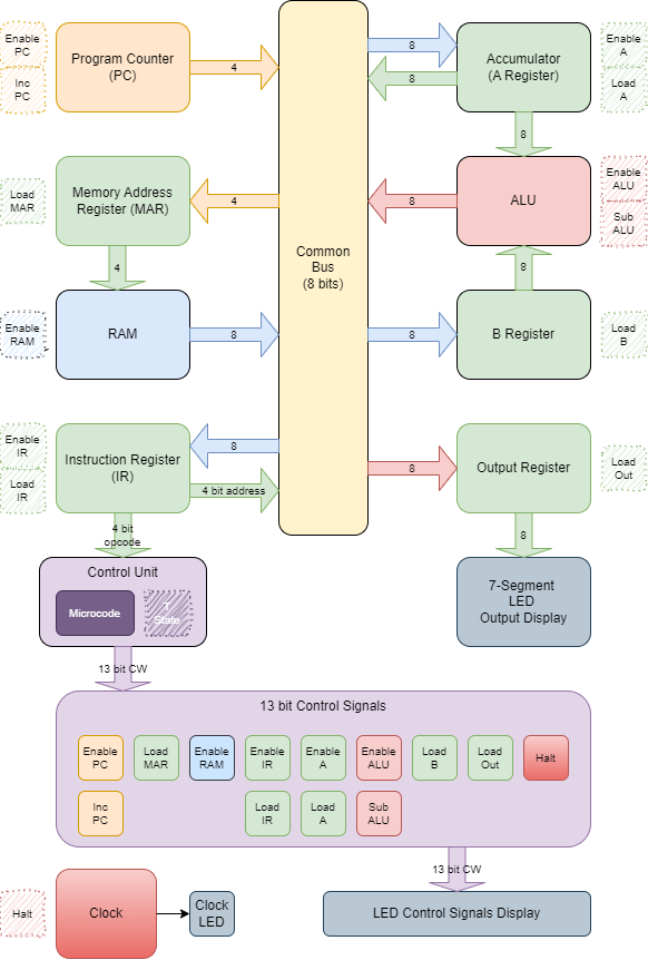
To implement Malvino’s SAP-1 (Simple As Possible) CPU in Verilog for the Nexys A7 AT-100 FPGA, we’ll need to break it down into components such as:
- Program Counter (PC): A simple counter to hold the address of the next instruction.
- Memory Address Register (MAR): Holds the address of the memory to fetch.
- Instruction Register (IR): Holds the instruction fetched from memory.
- Control Unit (CU): Controls the operation of other components based on the opcode in IR.
- Arithmetic Logic Unit (ALU): Performs arithmetic operations.
- Accumulator (ACC): Temporary register for holding the results of operations.
- Output Register (OUT): Holds the result to be output.
Here is a simplified architecture diagram of my understanding of SAP-1.
Clock
Overview
The Nexys A7 FPGA development board operates with a clock running at 100 MHz, which is too fast for us to meaningfully observe the state transitions in a simple SAP-1 architecture. Our goal is to slow the clock down to about 1 Hz so that we can visually track the state transitions. Furthermore, to assist in debugging and execution analysis, we need the ability to step through states manually.
To accomplish this, we use the following key features on the development board:
- 16 slide switches – One of these switches is dedicated to toggling between automatic slow clock mode and manual step mode.
- Push button – This button is used to manually advance the clock when in single-step mode.
- LED – We use an LED to indicate the clock pulse, allowing for visual confirmation of the clock’s operation. Since mechanical switches and buttons tend to produce noisy signals due to bouncing (brief unintended transitions), we implement debouncing to ensure reliable and stable clock control.
Key Requirements
- Slow the system clock: The 100 MHz clock is slowed down to 1 Hz using a clock divider, so that each state transition occurs every second.
- Manually advance the clock: In manual mode, we use a push button to advance the clock.
- Switch between automatic and manual clock modes: A slide switch toggles between the two modes.
- Halt the clock: A halt signal is used to stop the clock when the program completes.
- Reset the clock and debounce logic: The reset signal restores the clock to its default state and clears any pending signals.
- Visual clock pulse: An LED is driven by the clock signal to provide a visual cue of clock activity.
Inputs and Outputs
Inputs:
- clk_in: 100 MHz input clock from the Nexys A7 FPGA board.
- reset: A reset signal to reset the clock and debounce logic.
- mode_switch: A slide switch to select between automatic (slow clock) and manual (step-by-step) modes.
- step_button: A push button to manually step through the clock in manual mode.
- halt: A flag to stop the clock when the program execution is complete.
Output:
- clk_out: The output clock signal, either slowed down or advanced manually.
Internal Signals and Registers
- DIVISOR: A parameter set to 50,000,000, which divides the 100 MHz clock to approximately 1 Hz. debounced_step_button and debounced_mode_switch: Debounced signals from the button and slide switch, ensuring clean transitions.
- counter: A 32-bit counter used for clock division to achieve the slower clock frequency.
- slow_clk: A slow clock signal that toggles at 1 Hz.
- button_state_prev: Used to store the previous state of the step button for edge detection.
Debouncing the Button and Switch
Mechanical switches and buttons often produce multiple, unintended transitions due to bouncing. Without debouncing, the FPGA could interpret a single press as multiple presses, causing unreliable behavior. To prevent this, we use a debounce module to filter out the noise.
The debounce module uses a parameter DEBOUNCE_TIME to define the time required to stabilize the signal, ensuring only one clean transition is registered when a button is pressed or a switch is toggled.
Clock Divider for Slow Clock Mode
The input clock (clk_in) runs at 100 MHz, which is too fast for observing state transitions. To slow this down, we use a clock divider that counts clock cycles and toggles the clock output (slow_clk) when the count reaches DIVISOR - 1. This produces a clock signal that runs at 1 Hz, meaning each clock pulse occurs every second.
Clock Output Logic
The clock output logic determines whether the system is in single-step mode or slow clock mode:
- Single-Step Mode: When the mode_switch is high, the system waits for a button press to advance the clock. The clock only toggles on the rising edge of the step_button.
- Slow Clock Mode: When the mode_switch is low, the clock toggles automatically based on the slower clock (slow_clk) generated by the clock divider.
Reset and Halt Functionality
The reset signal is used to restore the clock to its initial state and clear any pending signals. The halt flag allows us to stop the clock when the system needs to halt, such as when the computer completes its program.
Visual Clock Pulse
To provide a visual indication of the clock pulse, we can connect an LED to the clk_out signal. This allows us to visually observe each clock pulse, making it easier to follow the clock transitions in real time.
Verilog Code for Clock
module clock (
    input wire clk_in,        // Input clock (100 MHz from Nexys A7-100)
    input wire reset,         // Reset signal
    input wire mode_switch,   // Slide switch for single-step (1) or slow clock (0)
    input wire step_button,   // Push button for single-step mode
    input wire halt,          // halt flag to end the program
    output reg clk_out        // Output clock (slowed or single-step)
);

    parameter DIVISOR = 50000000;  // Parameter to slow the clock (adjustable)
    wire debounced_step_button;    // Debounced button signal
    wire debounced_mode_switch;    // Debounced slide switch

    reg [31:0] counter = 0;        // 32-bit counter for clock division
    reg slow_clk = 0;              // Internal slow clock signal
    reg button_state_prev = 0;     // Previous state of the button

    // Instantiate the debounce module for the step button
    debounce #(.DEBOUNCE_TIME(100000)) debounce_step (
        .clk(clk_in),
        .reset(reset),
        .noisy_signal(step_button),
        .debounced_signal(debounced_step_button)
    );

    // Instantiate the debounce module for the mode switch
    debounce #(.DEBOUNCE_TIME(100000)) debounce_mode (
        .clk(clk_in),
        .reset(reset),
        .noisy_signal(mode_switch),
        .debounced_signal(debounced_mode_switch)
    );

    // Clock Divider: Generates the slow clock
    always @(posedge clk_in or posedge reset) begin
        if (reset) begin
            counter <= 0;
            slow_clk <= 0;
        end else begin
            if (counter >= (DIVISOR - 1)) begin
                counter <= 0;
                slow_clk <= ~slow_clk;  // Toggle the slow clock
            end else begin
                counter <= counter + 1;
            end
        end
    end

    // Single-Step Mode or Slow Clock Output Logic
    always @(posedge clk_in or posedge reset) begin
        if (reset) begin
            clk_out <= 0;
            button_state_prev <= 0;
        end else begin
            if (debounced_mode_switch) begin
                // Single-step mode: clock toggles only on rising edge of debounced button
                if (debounced_step_button && ~button_state_prev) begin
                    clk_out <= (halt) ? 0 : ~clk_out;
                end
            end else begin
                // Slow clock mode: use the divided slow clock
                clk_out <= (halt) ? 0 : slow_clk;
            end
            button_state_prev <= debounced_step_button; // Store the previous button state
        end
    end

endmodule
Constraints Definition
## Clock signal
set_property -dict { PACKAGE_PIN E3    IOSTANDARD LVCMOS33 } [get_ports { clk_in }]; #IO_L12P_T1_MRCC_35 Sch=clk100mhz
create_clock -add -name sys_clk_pin -period 10.00 -waveform {0 5} [get_ports {clk_in}];
##Switches
set_property -dict { PACKAGE_PIN V10   IOSTANDARD LVCMOS33 } [get_ports { mode_switch }]; #IO_L21P_T3_DQS_14 Sch=sw[15]
## LEDs
set_property -dict { PACKAGE_PIN V11   IOSTANDARD LVCMOS33 } [get_ports { clk_led }]; #IO_L21N_T3_DQS_A06_D22_14 Sch=led[15]
##Buttons
set_property -dict { PACKAGE_PIN M18   IOSTANDARD LVCMOS33 } [get_ports { step_button }]; #IO_L4N_T0_D05_14 Sch=btnu
set_property -dict { PACKAGE_PIN P17   IOSTANDARD LVCMOS33 } [get_ports { reset }]; #IO_L12P_T1_MRCC_14 Sch=btnl
Verilog Code for Debouncing Switches
module debounce (
    input wire clk,           // System clock (e.g., 100 MHz)
    input wire reset,         // Reset signal
    input wire noisy_signal,  // Noisy input signal (button press)
    output reg debounced_signal // Debounced output signal
);

    parameter DEBOUNCE_TIME = 100000; // Debounce time in clock cycles

    reg [31:0] debounce_counter = 0; // Counter to track signal stability
    reg stable_signal = 0;           // Stable signal before debouncing

    // Debounce Logic
    always @(posedge clk or posedge reset) begin
        if (reset) begin
            debounce_counter <= 0;
            debounced_signal <= 0;
            stable_signal <= 0;
        end else begin
            if (noisy_signal == stable_signal) begin
                debounce_counter <= 0; // No change in signal, reset counter
            end else begin
                // Signal has changed, start counting
                if (debounce_counter >= DEBOUNCE_TIME) begin
                    stable_signal <= noisy_signal; // Signal stable for long enough
                    debounced_signal <= noisy_signal;
                    debounce_counter <= 0;
                end else begin
                    debounce_counter <= debounce_counter + 1; // Increment counter
                end
            end
        end
    end

endmodule
Program Counter
Overview
The Program Counter (PC) is a critical component in any CPU, including the SAP-1 architecture. Its role is to keep track of the address of the next instruction to be executed. In this case, the PC is a 4-bit counter, which means it can store values from 0 to 15 (in binary, 4 bits). Each time the clock signal (clk) ticks, the PC can either increment by 1 or reset to 0 if needed.
Inputs and Outputs
Inputs:
- clk: The clock signal, which controls when the PC updates.
- reset: A signal to reset the PC to 0.
- inc: An increment signal. When inc is high, the PC increments by 1.
Output:
- pc_out: The 4-bit output value of the Program Counter. It holds the current address of the next instruction.
Functionality
Reset and Increment
- Reset (reset): When the reset signal is active (1), the PC is reset to 0. This ensures that the Program Counter starts from the first instruction of the program, typically during initialization or when a system reset is triggered.
- Increment (inc): The inc signal is used to increment the PC. When inc is active (1), the PC increases by 1 on each rising edge of the clock (clk), but only if the current PC value is less than 15 (4’b1111). This prevents the counter from overflowing since it is only 4 bits wide. Once it reaches 15, it will stop incrementing.
Key Points
- Clock Signal (clk): The Program Counter updates on every rising edge of the clock signal. This is typical in digital circuits to ensure that updates occur synchronously with the clock.
- Reset Mechanism: The pc_out is set to 0 whenever the reset signal is active. This ensures that the counter starts from the beginning of the program execution or when a reset is required.
- Conditional Increment: The Program Counter only increments if the inc signal is high and the current value of pc_out is less than 15 (4’b1111). This guarantees that the PC does not overflow past its 4-bit limit, ensuring it stays within the range 0-15.
Application in SAP-1
In the SAP-1 architecture, the Program Counter is essential for stepping through instructions stored in memory. Each instruction is fetched from memory using the current value of the Program Counter (pc_out), which is then incremented to point to the next instruction. The ability to reset and control the PC makes it easier to manage program flow during execution, particularly when debugging or running test programs.
Verilog Code for Program Counter
module pc (
    input wire clk,
    input wire reset,
    input wire inc,
    output reg [3:0] pc_out
);
    always @(posedge clk or posedge reset) begin
        if (reset)
            pc_out <= 4'b0;
        else if (inc && pc_out < 4'b1111)
            pc_out <= pc_out + 1;
    end
endmodule
Memory (RAM)
Overview
The memory module simulates the RAM (Random Access Memory) in the SAP-1 architecture. In this design, the memory holds the program instructions and data that the CPU will execute. It has 16 addresses, each storing 8 bits of data, which is typical for small, simple processors like the SAP-1. This module is essential for storing both the program instructions and the data that the CPU will process.
Inputs and Outputs
Inputs:
- address: A 4-bit address input that specifies which memory location to access. Since it’s a 4-bit address, there are 16 possible memory locations (2^4 = 16).
Outputs:
- data_out: An 8-bit output that provides the data stored at the given address. This data could represent either an instruction (for the CPU to execute) or data to be used in a computation.
Functionality
Memory Array
The memory is defined as a 16-byte array (ram), where each location holds 8 bits of data. This memory holds both the program instructions and data used by the processor. The memory is initialized with both instructions and data values at specific addresses.
- Instructions: These are the first few locations in memory (addresses 0 to 4). They form a small example program that the CPU can execute:
- ram[0] = 8’b00011110; — Load the value from memory location 14 (LDA 14).
- ram[1] = 8’b00101111; — Add the value from memory location 15 (ADD 15).
- ram[2] = 8’b00111101; — Subtract the value from memory location 13 (SUB 13).
- ram[3] = 8’b01000000; — Output the result to the output register (OUT).
- ram[4] = 8’b11110000; — Halt the CPU (HLT).
- NOP (No Operation): The program includes several NOPs (No Operation), which are instructions that do nothing. These are placeholders in memory locations 5 to 12.
- Data: Memory locations 13, 14, and 15 store the data used by the program:
- ram[13] = 8’b00000010; — Stores the value 2.
- ram[14] = 8’b00000110; — Stores the value 6.
- ram[15] = 8’b00000101; — Stores the value 5.
Output Logic
Memory Access: Whenever the CPU provides an address via the address input, the module outputs the corresponding data via data_out. The data_out register is updated with the data stored at the given address in the memory array.
Key Points
- Memory Initialization: The initial block pre-loads the memory with both instructions and data before the simulation or operation starts. This is useful for testing and running small programs within the SAP-1 CPU.
- Program Structure: The program consists of a series of instructions (like LDA, ADD, SUB, OUT, and HLT) that the CPU will execute in sequence. These instructions manipulate the data stored in other memory locations.
- Simple Addressing: The memory uses a 4-bit address (address), which allows the CPU to access any of the 16 memory locations. Each memory location holds an 8-bit value (data_out).
Application in SAP-1
In the SAP-1 architecture, this memory module is used to store both the program instructions and the data the CPU needs to process. The Program Counter (PC) provides the memory address to this module, which in turn outputs the corresponding instruction or data. This is an essential part of how the CPU fetches and executes instructions from memory.
Verilog Code for Memory
module memory (
    input wire [3:0] address,
    output reg [7:0] data_out
);
    reg [7:0] ram [0:15]; // 16 bytes of memory

    initial begin
        // Example program
        ram[0]  = 8'b00011110; // LDA 14
        ram[1]  = 8'b00101111; // ADD 15
        ram[2]  = 8'b00111101; // SUB 13
        ram[3]  = 8'b01000000; // OUT
        ram[4]  = 8'b11110000; // HLT

        ram[5]  = 8'b00000000; // NOP
        ram[6]  = 8'b00000000; // NOP
        ram[7]  = 8'b00000000; // NOP
        ram[8]  = 8'b00000000; // NOP
        ram[9]  = 8'b00000000; // NOP
        ram[10]  = 8'b00000000; // NOP
        ram[11]  = 8'b00000000; // NOP
        ram[12]  = 8'b00000000; // NOP

        ram[13] = 8'b00000010; // Data at memory location value 2
        ram[14] = 8'b00000110; // Data at memory location value 6
        ram[15] = 8'b00000101; // Data at memory location value 5
    end

    always @(*) begin
        data_out = ram[address];
    end
endmodule
Registers
Accumulator - A Register
Overview
The A register is an essential part of the SAP-1 architecture. It serves as an accumulator, a common register used in many simple CPUs. The accumulator holds data that will be manipulated by arithmetic and logic operations, and stores the result of these operations. In this design, the A register can load data from an external source (e.g., memory or another register) and is updated on each clock cycle when required.
Inputs and Outputs
- Inputs:
- clk: The clock signal that drives the register’s operation.
- reset: A signal to reset the register’s output to zero.
- load: A control signal that, when high, allows the register to load new data.
- data_in: The 8-bit data input to be loaded into the register.
- Outputs:
- data_out: The 8-bit data output, which holds the current value of the register.
Functionality
The A register performs two main functions:
- Storing Data: It holds an 8-bit value, which can be loaded from the data_in input when the load signal is high.
- Resetting the Data: When the reset signal is activated (high), the register clears its output, setting data_out to 0.
- Reset Behavior
- If the reset signal is high during a clock cycle, the register output (data_out) is immediately reset to 0.
- Load Data Behavior
- If the reset signal is not active, and the load signal is high, the register loads the data from data_in into data_out on the rising edge of the clock signal.
- Reset Behavior
Key Points
- Reset Functionality:
- When the reset signal is high, the register output data_out is cleared to 0 on the rising edge of the clock.
- This ensures that the register can be cleared and ready for new operations.
- Data Load Control:
- The load signal controls when new data is loaded into the register.
- When load is high during a clock cycle, the value from data_in is transferred to data_out.
- Clock-Synchronized Operation:
- The register is edge-triggered, meaning that it updates its value only on the rising edge of the clock (clk).
- This ensures that the operations are synchronized with the rest of the system.
Application in SAP-1
In the SAP-1 architecture, the A register serves as the accumulator. It stores data used in arithmetic operations like addition or subtraction. It holds the operand fetched from memory or the result of computations, making it a vital component in the processor’s operation. For example:
- When executing an LDA instruction, the value from memory is loaded into the A register via data_in.
- When performing an ADD instruction, the A register holds one operand, while the other comes from memory or another register. The result of the addition is stored back in the A register.
The reset signal allows the register to be cleared, and the load signal controls when new data is loaded into the A register.
Verilog code for A Register
module a (
    input wire clk,
    input wire reset,
    input wire load,
    input wire [7:0] data_in,
    output reg [7:0] data_out
);
    always @(posedge clk or posedge reset) begin
        if (reset)
            data_out <= 8'b0;
        else if (load)
            data_out <= data_in;
    end
endmodule
B Register
Overview
The B register in the SAP-1 architecture is another general-purpose register, much like the A register, but with a specific role during arithmetic operations. The B register typically holds the second operand in arithmetic operations such as addition or subtraction. In this simple CPU design, it temporarily stores data to be used in conjunction with the value in the A register.
Inputs and Outputs
- Inputs:
- clk: The clock signal that drives the register’s operations.
- reset: A signal to reset the register’s output to zero.
- load: A control signal that, when high, allows the register to load new data.
- data_in: The 8-bit data input to be loaded into the register.
- Outputs:
- data_out: The 8-bit data output, which holds the current value of the register.
Functionality
The B register performs two main functions:
- Storing Data: It holds an 8-bit value, which can be loaded from the data_in input when the load signal is high.
- Resetting the Data: When the reset signal is activated (high), the register clears its output, setting data_out to 0.
- Reset Behavior
- If the reset signal is high during a clock cycle, the register output (data_out) is immediately reset to 0.
- Load Data Behavior
- If the reset signal is not active, and the load signal is high, the register loads the data from data_in into data_out on the rising edge of the clock signal.
Key Points
- Reset Functionality:
- When the reset signal is high, the register output data_out is cleared to 0 on the rising edge of the clock.
- This ensures that the register can be cleared and ready for new operations.
- Data Load Control:
- The load signal controls when new data is loaded into the register.
- When load is high during a clock cycle, the value from data_in is transferred to data_out.
- Clock-Synchronized Operation:
- The register is edge-triggered, meaning that it updates its value only on the rising edge of the clock (clk).
- This ensures that the operations are synchronized with the rest of the system.
Application in SAP-1
In the SAP-1 architecture, the B register works in tandem with the A register during arithmetic operations. While the A register holds the primary operand (or the result of operations), the B register stores the secondary operand, typically fetched from memory.
For example:
- During an ADD operation, the value in the A register is added to the value in the B register, and the result is stored back in the A register.
- During a SUB operation, the B register holds the value to be subtracted from the A register.
This register is essential for performing two-operand arithmetic, and its functionality is critical for basic ALU operations in the SAP-1 CPU.
Verilog code for B Register
module b (
    input wire clk,
    input wire reset,
    input wire load,
    input wire [7:0] data_in,
    output reg [7:0] data_out
);
    always @(posedge clk or posedge reset) begin
        if (reset)
            data_out <= 8'b0;
        else if (load)
            data_out <= data_in;
    end
endmodule
Memory Address Register (MAR)
Overview
The Memory Address Register (MAR) in the SAP-1 architecture holds the address of the memory location that is currently being accessed. It is a critical component in the fetch-decode-execute cycle, responsible for pointing to the next instruction or data in memory. The MAR ensures that the correct address is supplied to the memory during read or write operations.
Inputs and Outputs
- Inputs:
- clk: The clock signal that drives the register’s operations.
- reset: A signal to reset the register’s output to zero.
- load: A control signal that, when high, allows the register to load a new memory address.
- address_in: The 4-bit address input to be loaded into the register.
- Outputs:
- address_out: The 4-bit address output, representing the current memory address stored in the MAR.
Functionality
The Memory Address Register (MAR) is a simple register that holds a 4-bit address used to point to a memory location. The MAR loads the new address from the address_in input when the load signal is high and can be reset to zero using the reset signal. This register plays a vital role in accessing instructions or data stored in memory.
Reset Behavior
- If the reset signal is high during a clock cycle, the MAR output (address_out) is immediately set to 0. This clears the memory address, ensuring that the system starts fresh during reset.
Load Address Behavior
- If the reset signal is not active and the load signal is high, the MAR loads the value from address_in into address_out on the rising edge of the clock. This address is then used to access a memory location in the next step of the instruction cycle.
Key Points
- Reset Functionality:
- When the reset signal is high, the register output address_out is cleared to 0 on the rising edge of the clock. This is useful when restarting the program or resetting the system.
- Address Load Control:
- The load signal controls when the new memory address from address_in is loaded into address_out.
- When load is high during a clock cycle, the address from address_in is transferred to address_out, and this address is used to access the appropriate memory location.
- Clock-Synchronized Operation:
- The register is edge-triggered, meaning that it updates its value only on the rising edge of the clock (clk).
- This ensures that the operations are synchronized with the rest of the system, ensuring proper timing in the CPU’s fetch-decode-execute cycle.
Application in SAP-1
In the SAP-1 architecture, the Memory Address Register (MAR) is used to hold the address of the memory location being accessed for fetching instructions or data. During the fetch stage of the instruction cycle, the MAR is loaded with the next instruction address. The address stored in the MAR is used to retrieve the instruction from memory, which is then executed by the CPU.
For example:
- During the fetch phase, the program counter (PC) provides the address of the next instruction. This address is loaded into the MAR.
- The memory module uses the address from the MAR to retrieve the instruction from memory.
The MAR is essential for addressing memory locations and plays a key role in ensuring that instructions are fetched and executed in the correct order.
Verilog code for Memory Address Register (MAR)
module mar(
    input wire clk,
    input wire reset,
    input wire load,
    input wire [3:0] address_in,
    output reg [3:0] address_out
);
    always @(posedge clk, posedge reset) begin
        if (reset) begin
            address_out <= 4'b0;
        end else if (load) begin
            address_out <= address_in;
        end
    end

endmodule
Instruction Register (IR)
Overview
The Instruction Register (IR) in the SAP-1 architecture holds the current instruction that the CPU is executing. It splits the instruction into two parts: the opcode (the operation to perform) and the operand (the data or address associated with the operation). The IR plays a critical role in controlling the CPU’s execution flow by interpreting and storing instructions fetched from memory.
Inputs and Outputs
- Inputs:
- clk: The clock signal that synchronizes the register’s operations.
- reset: A signal to reset the instruction register to zero.
- load: A control signal that, when high, loads a new instruction into the IR.
- instruction_in: The 8-bit input representing the instruction to be loaded.
- Outputs:
- opcode: The 4-bit output representing the operation part of the instruction.
- operand: The 4-bit output representing the data or address part of the instruction.
Functionality
The Instruction Register (IR) takes an 8-bit instruction input (instruction_in) and splits it into two 4-bit parts:
- The opcode (higher 4 bits) specifies the operation the CPU should perform.
- The operand (lower 4 bits) provides the data or memory address for the operation.
Reset Behavior
- If the reset signal is high during a clock cycle, both opcode and operand are reset to 0, ensuring that no previous instruction remains in the register when the system is restarted.
Load Instruction Behavior
- If the load signal is high during the clock cycle, the IR loads the 8-bit instruction_in into its opcode and operand fields. The 4 most significant bits are stored in opcode, while the 4 least significant bits are stored in operand.
Key Points
- Reset Functionality:
- When the reset signal is high, both the opcode and operand are cleared to 0. This ensures that no previous instruction remains in the IR after a reset event, such as restarting the CPU or clearing the current state.
- Instruction Loading:
- When the load signal is high, the 8-bit instruction_in is split into the opcode (higher 4 bits) and operand (lower 4 bits) on the rising edge of the clock.
- The opcode determines what operation will be executed (e.g., ADD, SUB, LDA, etc.), while the operand provides the associated data or memory address for that operation.
- Clock-Synchronized Operation:
- The IR updates its values only on the rising edge of the clock (clk). This ensures that the register operates in sync with the rest of the system, allowing the fetch-decode-execute cycle to proceed smoothly.
Application in SAP-1
In the SAP-1 architecture, the Instruction Register (IR) is loaded with the instruction fetched from memory during the fetch phase. Once loaded, the instruction is split into:
- The opcode: This tells the control unit which operation to perform (e.g., ADD, SUB, HLT).
- The operand: This provides the memory address or data value needed for the operation.
For example, in a simple program: The instruction 8’b00101111 (binary) could be decoded as:
- Opcode: 0010 (binary) → ADD operation
- Operand: 1111 (binary) → Memory address or data value for the ADD operation
During the fetch-decode-execute cycle:
- The IR first holds the instruction fetched from memory.
- The control unit then decodes the opcode and operand, determining the next operation to perform.
This register is vital for orchestrating the correct execution of instructions, ensuring that the CPU operates according to the program stored in memory.
Verilog code for Instruction Register (IR)
module ir (
    input wire clk,
    input wire reset,
    input wire load,
    input wire [7:0] instruction_in,
    output reg [3:0] opcode,
    output reg [3:0] operand
);

    initial begin
        opcode = 4'b0;
        operand = 4'b0;
    end

    always @(posedge clk, posedge reset) begin
        if (reset) begin
            opcode <= 4'b0;
            operand <= 4'b0;
        end else if (load) begin
            opcode <= instruction_in[7:4];
            operand <= instruction_in[3:0];
        end
    end
endmodule
Output Register
Overview
The Output Register (OUT) in the SAP-1 architecture is responsible for holding and displaying the result of computations performed by the CPU. It stores an 8-bit value and outputs it to a display device (e.g., LEDs or a seven-segment display). The value in the output register remains constant until a new value is loaded, which allows the system to visualize the result of the executed instructions.
Inputs and Outputs
- Inputs:
- clk: The clock signal to synchronize the register’s operations.
- reset: A signal to reset the output register to zero.
- load: A control signal that, when high, loads new data into the output register.
- data_in: The 8-bit input data to be loaded into the output register.
- Outputs:
- data_out: The 8-bit output representing the value stored in the output register. This value is displayed or sent to an external device.
Functionality
The Output Register (OUT) takes an 8-bit input (data_in) and stores it in the register when the load signal is high. This stored value is continuously output as data_out, providing the final result of the computation or operation. The output remains unchanged until new data is loaded into the register.
Reset Behavior
- If the reset signal is high during a clock cycle, the output (data_out) is cleared to 0. This ensures that the output register starts from a known state when the system is reset.
Load Data Behavior
- If the load signal is high during a clock cycle, the 8-bit data_in is stored in the output register, and this value is subsequently available on the data_out output.
Key Points
- Reset Functionality:
- When the reset signal is high, the data_out is cleared to 0. This ensures that the output register is in a known state when the system is reset, and no stale data is left in the register.
- Data Loading:
- When the load signal is high, the 8-bit data_in is stored in the data_out register. This value is then available for display or output, making it visible on the LEDs or connected display devices.
- The loaded value remains on the data_out output until another load operation or a reset occurs.
- Clock-Synchronized Operation:
- The register updates only on the rising edge of the clock (clk). This ensures that the output register’s operation is synchronized with the rest of the system, and that new values are loaded at the correct time within the CPU’s clock cycle.
Application in SAP-1
In the SAP-1 architecture, the Output Register (OUT) holds the result of arithmetic and logic operations. After a computation, the value from the accumulator (A) or other registers is transferred to the output register to be displayed.
For example:
- After performing an ADD or SUB operation, the result in the accumulator can be loaded into the output register for visualization.
- The system’s external components, such as a display, will show the value stored in the output register, allowing the user to see the result of the executed instruction.
Example Workflow
- Reset: The system is reset, clearing the output register (data_out = 0).
- Operation Execution: The CPU performs a series of operations, and the result is available as data_in.
- Load New Data: When the load signal is high, the value of data_in is loaded into the output register, updating data_out.
- Output Display: The data_out value remains constant and is displayed on the connected device until a new value is loaded or a reset occurs.
Verilog code for Output Register
module out (
    input wire clk,
    input wire reset,
    input wire load,
    input wire [7:0] data_in,
    output reg [7:0] data_out
);
    always @(posedge clk or posedge reset) begin
        if (reset) begin
            data_out <= 1'b00000000;
        end else if (load) begin
            data_out <= data_in;
        end
    end
endmodule
Arithmetic and Logic Unit (ALU)
Overview
The Arithmetic Logic Unit (ALU) in the SAP-1 architecture is responsible for performing arithmetic operations on two 8-bit input values: a and b. Specifically, this ALU performs addition or subtraction based on a control signal. It is a simple ALU that handles two’s complement subtraction and unsigned addition.
Inputs and Outputs
- Inputs:
- a: The first 8-bit input to the ALU.
- b: The second 8-bit input to the ALU.
- sub: A control signal that determines whether the ALU performs addition or subtraction. If sub = 1, the ALU performs subtraction (a - b). If sub = 0, it performs addition (a + b).
- Output:
- result: The 8-bit result of the operation, either the sum or the difference of a and b.
Functionality
The ALU module performs one of two operations:
- Addition: When the sub signal is low (0), the ALU adds the two 8-bit inputs (a + b), and the result is stored in result.
- Subtraction: When the sub signal is high (1), the ALU subtracts b from a (a - b), and the result is stored in result.
The ALU does not handle overflow detection, and it treats both addition and subtraction as unsigned operations.
Key Points
- Addition and Subtraction:
- The ALU performs addition when the sub signal is 0, meaning it calculates result = a + b.
- It performs subtraction when the sub signal is 1, meaning it calculates result = a - b. The subtraction is done in two’s complement, ensuring correct results even when b is larger than a for signed operations.
- Combinational Logic:
- The ALU is a combinational circuit, meaning the result is calculated immediately based on the current values of the inputs (a, b, and sub). The result is always updated as soon as any of the inputs change.
- Unsigned Operations:
- This ALU does not handle signed numbers directly. It performs operations assuming that the inputs are unsigned, and no overflow detection is included. However, it can work correctly for two’s complement numbers in both addition and subtraction modes.
- Control Signal:
- The sub signal is the control input for the ALU. If sub = 0, the ALU performs addition; if sub = 1, it performs subtraction. This simple approach allows the ALU to handle both operations with minimal logic.
Application in SAP-1
In the SAP-1 architecture, the ALU is used to perform basic arithmetic operations such as addition and subtraction. These operations are essential for performing calculations based on instructions like ADD and SUB in the instruction set.
For example:
- The ADD instruction takes two values (from registers or memory) and adds them together using the ALU. The result is then stored in the accumulator or other registers.
- The SUB instruction subtracts one value from another, and the result is also stored.
Example Workflow
- Addition Operation:
- Inputs: a = 8’b00000101 (5), b = 8’b00000011 (3), and sub = 0 (addition).
- The ALU will compute a + b = 5 + 3 = 8, and store 8 in the result.
- Subtraction Operation:
- Inputs: a = 8’b00000101 (5), b = 8’b00000011 (3), and sub = 1 (subtraction).
- The ALU will compute a - b = 5 - 3 = 2, and store 2 in the result.
Example in SAP-1
The ALU can be used for the following operations in the SAP-1 system:
- ADD: The ALU adds the values in registers or memory and stores the result.
- SUB: The ALU subtracts one value from another and stores the result.
These operations are essential for performing calculations during program execution.
Verilog code for Arithmetic and Logic Unit (ALU)
module alu (
    input wire [7:0] a,
    input wire [7:0] b,
    input wire sub,
    output reg [7:0] result
);
    always @(*) begin
        if (sub)
            result = a - b;
        else
            result = a + b;
    end
endmodule
Control Sequencer
Overview
The controller module in the SAP-1 (Simple as Possible) architecture is responsible for generating the control signals based on the opcode and the T-state of the system. These control signals dictate the actions of other components (such as the program counter, memory, and registers) at specific stages of an instruction cycle.
Inputs and Outputs
- Inputs:
- clk: The system clock that drives the T-states and control sequence.
- reset: A signal to reset the state machine, bringing it back to the initial state.
- opcode: A 4-bit opcode that represents the current instruction to be executed.
- Outputs:
- cs: A 13-bit wide output representing the control signals for the entire system.
- tstate: A 3-bit value representing the current T-state (machine cycle step).
Supported Instructions (Opcodes)
The following instructions are defined for this controller:
- NOP: No operation (reset state).
- LDA: Load data into register A.
- ADD: Add data to register A.
- SUB: Subtract data from register A.
- OUT: Output data from register A.
- HLT: Halt the program.
These opcodes are mapped to 4-bit values to identify the instruction in the system.
Control Signals:
The module generates 13 control signals for various operations in the SAP-1 architecture, each controlling specific actions such as enabling components, loading data, and controlling the ALU:
Control signals include:
- LOAD_OUT: Load data into the output register.
- HALT: Stop the clock, halting the system.
- INC_PC: Increment the program counter.
- EN_PC: Enable the program counter to place its address on the bus.
- LOAD_MAR: Load the memory address register (MAR) with data from the bus.
- EN_RAM: Enable the memory to place its data onto the bus.
- LOAD_IR: Load the instruction register (IR) with data from the bus.
- EN_IR: Enable the instruction register (IR) to place its address onto the bus.
- LOAD_A: Load register A with data from the bus.
- EN_A: Enable register A to place its data on the bus.
- LOAD_B: Load register B with data from the bus.
- SUB_ALU: Signal the ALU to perform subtraction.
- EN_ALU: Enable the ALU to place its result on the bus.
T-State Breakdown
The T-state represents the microcode execution phase, breaking down each instruction into smaller steps. The controller moves through six T-states (0 through 5), controlling different actions at each step. These steps ensure that the instruction is fetched, decoded, and executed in sequence.
- T-State 0: Fetch the instruction from memory by loading the MAR with the address from the program counter (PC).
- T-State 1: Increment the PC so that it points to the next instruction.
- T-State 2: Load the instruction into the instruction register (IR).
- T-State 3-5: Execute the current instruction based on the opcode.
Each instruction has its specific control signals asserted during these T-states.
Control Signal Generation Based on Opcode
In T-states 3-5, the controller acts based on the current instruction (as identified by the opcode). The following logic is applied:
- NOP (No Operation): No action is performed during T-states 3-5.
- LDA (Load A):
- T-State 3: Load the memory address into MAR.
- T-State 4: Load the data from memory into register A.
- ADD:
- T-State 3: Load the memory address into MAR.
- T-State 4: Load the data from memory into register B.
- T-State 5: Add the contents of A and B, storing the result in A.
- SUB:
- T-State 3: Load the memory address into MAR.
- T-State 4: Load the data from memory into register B.
- T-State 5: Subtract the contents of B from A, storing the result in A.
- OUT:
- T-State 3: Load the contents of register A into the output register.
- HLT: Halt the system and stop the clock.
Example of Operation:
For the ADD instruction:
- T-State 0: The program counter places the current address on the bus, and the MAR loads this address.
- T-State 1: The program counter is incremented.
- T-State 2: The instruction is fetched from memory and placed in the IR.
- T-State 3: The IR places the memory address of the operand on the bus, and the MAR loads it.
- T-State 4: The operand is fetched from memory and loaded into register B.
- T-State 5: The ALU adds the contents of A and B, placing the result back in register A.
Control Word (CW) Assembly
The control word (cw) is a 13-bit register that assembles the control signals for each T-state and opcode. For every clock cycle, it dictates which operations are performed by asserting or de-asserting the control signals.
The controller module plays a central role in orchestrating the actions of the SAP-1 system by breaking down instructions into smaller steps using a combination of T-states and control signals. This enables the proper sequencing of memory fetches, arithmetic operations, and control flow, such as halting the system. The modular design allows flexibility in expanding or modifying control signals for different or more complex instructions.
Verilog code for Control Sequencer
module controller (
    input wire clk,
    input wire reset,
    input wire [3:0] opcode,    // opcode is 4 bits wide, 16 possible instructions
    output [12:0] cs,           // we have 13 bits of control signals
    output [2:0] tstate
);

    // These are the supported instruction
    // NOP is not part of the SAP-1
    // but added here to avoid confusion as
    // we set the opcode to 4'b0000 when a reset is triggered
    localparam OP_NOP = 4'b0000;        // no operation
    localparam OP_LDA = 4'b0001;        // LOAD A
    localparam OP_ADD = 4'b0010;        // ADD
    localparam OP_SUB = 4'b0011;        // SUB
    localparam OP_OUT = 4'b0100;        // OUT
    localparam OP_HLT = 4'b1111;        // HALT

    // Control signals are parameters
    localparam LOAD_OUT   = 12;
    localparam HALT       = 11;
    localparam INC_PC    = 10;
    localparam EN_PC     = 9;
    localparam LOAD_MAR  = 8;
    localparam EN_RAM    = 7;
    localparam LOAD_IR   = 6;
    localparam EN_IR     = 5;
    localparam LOAD_A    = 4;
    localparam EN_A      = 3;
    localparam LOAD_B    = 2;
    localparam SUB_ALU   = 1;
    localparam EN_ALU    = 0;

    // we have 6 T states that breaks down the opcode into microcodes
    // this is a machine cycle
    reg[2:0] t_state;

    always @(posedge clk, posedge reset) begin
        if (reset) begin
            t_state <= 0;
        end else begin
            if (t_state == 5) begin
                t_state <= 0;
            end else begin
                t_state <= t_state + 1;
            end
        end
     end

    // we need to assemble the control signals into cw and finally write it out
    reg[12:0] cw;

    // Define control signals for different instructions
    // These signals change based on the T state we are in
    always @(*) begin

        // we clear the control word first and
        cw = 13'b0000000000000;
        // then build it based on the opcode and T state

        case (t_state)
            0: begin
                // this state is independent of the opcode
                // we need to load the the instruction pointed by PC into MAR
                cw[EN_PC] = 1;       // PC writes to the BUS
                cw[LOAD_MAR] = 1;    // MAR loads from the BUS
            end
            1: begin
               // this state is independent of the opcode
               cw[INC_PC] = 1;     // increment PC for the next instruction
            end
            2: begin
                // this state is independent of the opcode
                // RAM is hard wired to MAR
                // we need to load the RAM's content into the IR
                cw[EN_RAM] = 1;     // RAM writes to the BUS
                cw[LOAD_IR] = 1;    // IR loads from the BUS
            end
            // IR has already split the opcode part the instruction stored in RAM
            // We need to now handle the remaining T states based on the opcode
            3: begin
                case (opcode)
                    OP_NOP: begin
                        // we don't have to do anything
                        // just waste this clock cycle
                    end
                    OP_LDA, OP_ADD, OP_SUB: begin
                        // the operand part of the IR points to the memory location
                        // we need to know which memory location that is
                        cw[EN_IR] = 1;      // IR's writes to the BUS
                        cw[LOAD_MAR] = 1;   // MAR loads from the BUS
                    end
                    OP_HLT: begin
                        // this is the end of the program and so we can stop the clock
                        cw[HALT] = 1;
                    end
                    OP_OUT: begin
                        cw[EN_A] = 1;
                        cw[LOAD_OUT] = 1;
                    end
                endcase
            end
            4: begin
                case (opcode)
                    OP_NOP, OP_OUT: begin
                        // we don't have to do anything
                        // just waste this clock cycle
                    end
                    OP_LDA: begin
                        cw[EN_RAM] = 1;     // RAM's writes to the BUS
                        cw[LOAD_A] = 1;     // A Register loads from the BUS
                    end
                    OP_ADD, OP_SUB: begin
                        cw[EN_RAM] = 1;     // RAM's writes to the BUS
                        cw[LOAD_B] = 1;     // B Register loads from the BUS
                    end
                    OP_HLT: begin
                        // since the clock was stopped in the previous T state
                        // the code should not even reach here for this opcode
                        cw[HALT] = 1;
                    end
                endcase
            end
            5: begin
                case (opcode)
                    OP_NOP, OP_OUT: begin
                        // we don't have to do anything
                        // just waste this clock cycle
                    end
                    OP_ADD: begin
                        cw[EN_ALU] = 1;     // ALU's writes to the BUS
                        cw[LOAD_A] = 1;     // A Register loads from the BUS
                    end
                    OP_SUB: begin
                        cw[SUB_ALU] = 1;    // Let ALU know that we need it to subtract and not add
                        cw[EN_ALU] = 1;     // ALU's writes to the BUS
                        cw[LOAD_A] = 1;     // A Register loads from the BUS
                    end
                    OP_HLT: begin
                        // since the clock was stopped in the previous T state
                        // the code should not even reach here for this opcode
                        cw[HALT] = 1;
                    end
                endcase
            end
        endcase
    end

    assign cs = cw;
    assign tstate = t_state;

endmodule
Constraints Definition
## LEDs
set_property -dict { PACKAGE_PIN H17   IOSTANDARD LVCMOS33 } [get_ports { cs_led[0] }]; #IO_L18P_T2_A24_15 Sch=led[0]
set_property -dict { PACKAGE_PIN K15   IOSTANDARD LVCMOS33 } [get_ports { cs_led[1] }]; #IO_L24P_T3_RS1_15 Sch=led[1]
set_property -dict { PACKAGE_PIN J13   IOSTANDARD LVCMOS33 } [get_ports { cs_led[2] }]; #IO_L17N_T2_A25_15 Sch=led[2]
set_property -dict { PACKAGE_PIN N14   IOSTANDARD LVCMOS33 } [get_ports { cs_led[3] }]; #IO_L8P_T1_D11_14 Sch=led[3]
set_property -dict { PACKAGE_PIN R18   IOSTANDARD LVCMOS33 } [get_ports { cs_led[4] }]; #IO_L7P_T1_D09_14 Sch=led[4]
set_property -dict { PACKAGE_PIN V17   IOSTANDARD LVCMOS33 } [get_ports { cs_led[5] }]; #IO_L18N_T2_A11_D27_14 Sch=led[5]
set_property -dict { PACKAGE_PIN U17   IOSTANDARD LVCMOS33 } [get_ports { cs_led[6] }]; #IO_L17P_T2_A14_D30_14 Sch=led[6]
set_property -dict { PACKAGE_PIN U16   IOSTANDARD LVCMOS33 } [get_ports { cs_led[7] }]; #IO_L18P_T2_A12_D28_14 Sch=led[7]
set_property -dict { PACKAGE_PIN V16   IOSTANDARD LVCMOS33 } [get_ports { cs_led[8] }]; #IO_L16N_T2_A15_D31_14 Sch=led[8]
set_property -dict { PACKAGE_PIN T15   IOSTANDARD LVCMOS33 } [get_ports { cs_led[9] }]; #IO_L14N_T2_SRCC_14 Sch=led[9]
set_property -dict { PACKAGE_PIN U14   IOSTANDARD LVCMOS33 } [get_ports { cs_led[10] }]; #IO_L22P_T3_A05_D21_14 Sch=led[10]
set_property -dict { PACKAGE_PIN T16   IOSTANDARD LVCMOS33 } [get_ports { cs_led[11] }]; #IO_L15N_T2_DQS_DOUT_CSO_B_14 Sch=led[11]
set_property -dict { PACKAGE_PIN V15   IOSTANDARD LVCMOS33 } [get_ports { cs_led[12] }]; #IO_L16P_T2_CSI_B_14 Sch=led[12]
Display
The development board has 8 seven-segment LEDs, which we would like to use to display the hexadecimal values of various signals such as the Program Counter, the Bus, the Memory Address Register (MAR), the RAM contents pointed to by the MAR, T States, and more.
We need to decode the hexadecimal values to drive the individual segments of the seven-segment LED displays. Additionally, a multiplexer is required to control each of the seven-segment displays. Since we are relying on persistence of vision, we will use the system clock to refresh the display.
7-Segment Decoder
A 7-segment display decoder converts a 4-bit binary number into signals that can light up the appropriate segments of a 7-segment display to show digits from 0 to F (hexadecimal). Here’s an explanation of its components:
Inputs and Outputs:
- Inputs
- digit: A 4-bit input representing a hexadecimal digit (0-15).
- Outputs
- seg: A 7-bit output where each bit corresponds to one of the segments (A-G) of the display. The bits are:
- seg[6]: Segment A
- seg[5]: Segment B
- seg[4]: Segment C
- seg[3]: Segment D
- seg[2]: Segment E
- seg[1]: Segment F
- seg[0]: Segment G
- seg: A 7-bit output where each bit corresponds to one of the segments (A-G) of the display. The bits are:
Each bit is active low, meaning that a 0 lights up the corresponding segment, and a 1 turns it off.
Functionality:
The decoder uses a case statement to map each 4-bit input (digit) to the correct 7-bit output (seg). The binary output patterns represent which segments of the display should be lit up to show the corresponding digit.
Example Mapping:
- For digit = 4’d0 (binary 0000), the output is 7’b1000000, which lights up segments A, B, C, D, E, and F to display 0.
- For digit = 4’d1 (binary 0001), the output is 7’b1111001, lighting up segments B and C to display 1.
- For digit = 4’d10 (binary 1010), the output is 7’b0001000, which lights up segments A, B, C, E, and F to display A in hexadecimal.
The default case (when an invalid input is given) turns off all segments by setting the output to 7’b1111111.
Key Points:
- Hexadecimal Digits: The module supports hexadecimal digits, meaning it can display values from 0 (0000) to F (1111) on a 7-segment display.
- Efficient Case Statement: The module uses a case statement that ensures a direct mapping from each digit to its corresponding segment configuration.
- Default Behavior: If the input is outside the expected range (0-15), all segments are turned off, ensuring the display remains blank.
This decoder can be useful for systems that display numbers, letters (A-F), or for debugging purposes where hexadecimal values need to be displayed.
Verilog Code for 7-Segment Decoder
module seven_seg_decoder (
    input [3:0] digit,   // 4-bit input digit (0-15 for hex)
    output reg [6:0] seg // 7-segment display output (A-G)
);

always @(*) begin
    case (digit)
        4'd0: seg = 7'b1000000;  // Display 0
        4'd1: seg = 7'b1111001;  // Display 1
        4'd2: seg = 7'b0100100;  // Display 2
        4'd3: seg = 7'b0110000;  // Display 3
        4'd4: seg = 7'b0011001;  // Display 4
        4'd5: seg = 7'b0010010;  // Display 5
        4'd6: seg = 7'b0000010;  // Display 6
        4'd7: seg = 7'b1111000;  // Display 7
        4'd8: seg = 7'b0000000;  // Display 8
        4'd9: seg = 7'b0010000;  // Display 9
        4'd10: seg = 7'b0001000; // Display A
        4'd11: seg = 7'b0000011; // Display B
        4'd12: seg = 7'b1000110; // Display C
        4'd13: seg = 7'b0100001; // Display D
        4'd14: seg = 7'b0000110; // Display E
        4'd15: seg = 7'b0001110; // Display F
        default: seg = 7'b1111111;  // Turn off all segments
    endcase
end

endmodule
7-Segment Multiplexer
The seven-segment display multiplexer (MUX) module you’ve provided allows for displaying a 32-bit value across eight 7-segment displays. The core functionality is to multiplex the display, meaning it switches rapidly between digits so that all eight digits appear to be displayed simultaneously, even though only one is actually being lit at a time.
Inputs and Outputs:
- Inputs
- clk: The clock signal used for synchronizing the multiplexing process.
- reset: A reset signal that sets the system back to its initial state.
- value: A 32-bit value, containing eight 4-bit digits to display.
- Outputs
- an: The 8-bit output controlling the anodes of the 7-segment displays. A 0 in any bit of an enables the corresponding display.
- digit: The 4-bit output corresponding to the digit currently being displayed.
Key Components:
- Refresh Counter:
- A 20-bit refresh counter is used to create a slower refresh rate for the display multiplexing. The clock signal is divided down, and the most significant bits (refresh_counter[19:17]) control which digit to display. The counter allows for refreshing the display quickly enough to give the appearance that all digits are shown simultaneously.
- Digit Splitting:
- The 32-bit input value is split into eight 4-bit segments (digit0 through digit7), where each segment corresponds to a specific digit to be displayed on one of the 7-segment displays:
- digit0: Right-most digit.
- digit7: Left-most digit.
- The 32-bit input value is split into eight 4-bit segments (digit0 through digit7), where each segment corresponds to a specific digit to be displayed on one of the 7-segment displays:
- Multiplexing Logic:
- The multiplexing process is controlled by the refresh_digit signal (which is derived from refresh_counter[19:17]). This 3-bit signal determines which digit to display at any given moment.
- The an output enables one digit at a time by setting one bit of the 8-bit anode signal low (active low), while the others remain high (inactive). For example:
- an = 8’b11111110: The right-most digit (digit0) is enabled.
- an = 8’b01111111: The left-most digit (digit7) is enabled.
- Case Statement:
- The case statement maps each value of refresh_digit to the appropriate digit to display. This ensures that the correct 4-bit segment of the value is shown at the right time:
- When refresh_digit = 3’b000, it displays digit0.
- When refresh_digit = 3’b111, it displays digit7.
- The case statement maps each value of refresh_digit to the appropriate digit to display. This ensures that the correct 4-bit segment of the value is shown at the right time:
Functionality Overview:
- Clock-Driven Multiplexing:
- The display switches between the digits in a round-robin fashion, using the refresh counter to cycle through the digits.
- Even though only one digit is enabled at a time, the switching is fast enough that all eight digits appear to be displayed simultaneously.
- Reset Functionality:
- On reset, the refresh counter is set to zero, and all anodes are disabled (an = 8’b11111111), ensuring that no digits are displayed.
Key Points:
- Efficiency: The module only uses one active digit at a time, significantly reducing power consumption.
- Scalability: The design can handle 8 digits by simply cycling through the anodes, which is enough to display a 32-bit number (each digit representing 4 bits).
- Clock Sensitivity: The refresh rate is determined by the clock input. The module operates at a speed where all digits appear to be constantly illuminated.
This is an efficient design for 7-segment displays that need to show large numbers (like 32-bit values), and it can be used in many projects requiring visual feedback from microcontrollers, FPGA, or other digital systems.
Verilog Code for 7-Segment Multiplexer
module seven_seg_mux (
    input clk,                // Clock input
    input reset,              // Reset signal
    input [31:0] value,       // 32-bit value containing 8 digits
    output reg [7:0] an,      // Anodes for the 8 digits
    output reg [3:0] digit    // Current digit to display
);

reg [19:0] refresh_counter = 0;   // Refresh counter for multiplexing
wire [2:0] refresh_digit;         // Current digit being refreshed

// Split the 32-bit value into eight 4-bit digits
wire [3:0] digit0 = value[3:0];    // Right-most digit
wire [3:0] digit1 = value[7:4];    // Second digit
wire [3:0] digit2 = value[11:8];   // Third digit
wire [3:0] digit3 = value[15:12];  // Fourth digit
wire [3:0] digit4 = value[19:16];  // Fifth digit
wire [3:0] digit5 = value[23:20];  // Sixth digit
wire [3:0] digit6 = value[27:24];  // Seventh digit
wire [3:0] digit7 = value[31:28];  // Left-most digit

// Refresh rate for multiplexing the display (e.g., 1kHz)
always @(posedge clk or posedge reset) begin
    if (reset)
        refresh_counter <= 0;
    else
        refresh_counter <= refresh_counter + 1;
end

// The current digit to display (multiplexed)
assign refresh_digit = refresh_counter[19:17]; // Change every few clock cycles

// Multiplex the anodes and assign the current digit based on the refresh_digit
always @(*) begin
    if (reset) begin
        an = 8'b11111111;   // Disable all digits during reset
        digit = 4'b0000;    // Set all digits to zero
    end else begin
        case (refresh_digit)
            3'b000: begin
                an = 8'b11111110;   // Enable the right-most digit (digit 0)
                digit = digit0;
            end
            3'b001: begin
                an = 8'b11111101;   // Enable the second digit (digit 1)
                digit = digit1;
            end
            3'b010: begin
                an = 8'b11111011;   // Enable the third digit (digit 2)
                digit = digit2;
            end
            3'b011: begin
                an = 8'b11110111;   // Enable the fourth digit (digit 3)
                digit = digit3;
            end
            3'b100: begin
                an = 8'b11101111;   // Enable the fifth digit (digit 4)
                digit = digit4;
            end
            3'b101: begin
                an = 8'b11011111;   // Enable the sixth digit (digit 5)
                digit = digit5;
            end
            3'b110: begin
                an = 8'b10111111;   // Enable the seventh digit (digit 6)
                digit = digit6;
            end
            3'b111: begin
                an = 8'b01111111;   // Enable the left-most digit (digit 7)
                digit = digit7;
            end
            default: begin
                an = 8'b11111111;   // Disable all digits
                digit = 4'b0000;
            end
        endcase
    end
end

endmodule
Constraints Definition
##7 segment display
set_property -dict { PACKAGE_PIN T10   IOSTANDARD LVCMOS33 } [get_ports { seg[0] }]; #IO_L24N_T3_A00_D16_14 Sch=ca
set_property -dict { PACKAGE_PIN R10   IOSTANDARD LVCMOS33 } [get_ports { seg[1] }]; #IO_25_14 Sch=cb
set_property -dict { PACKAGE_PIN K16   IOSTANDARD LVCMOS33 } [get_ports { seg[2] }]; #IO_25_15 Sch=cc
set_property -dict { PACKAGE_PIN K13   IOSTANDARD LVCMOS33 } [get_ports { seg[3] }]; #IO_L17P_T2_A26_15 Sch=cd
set_property -dict { PACKAGE_PIN P15   IOSTANDARD LVCMOS33 } [get_ports { seg[4] }]; #IO_L13P_T2_MRCC_14 Sch=ce
set_property -dict { PACKAGE_PIN T11   IOSTANDARD LVCMOS33 } [get_ports { seg[5] }]; #IO_L19P_T3_A10_D26_14 Sch=cf
set_property -dict { PACKAGE_PIN L18   IOSTANDARD LVCMOS33 } [get_ports { seg[6] }]; #IO_L4P_T0_D04_14 Sch=cg
set_property -dict { PACKAGE_PIN H15   IOSTANDARD LVCMOS33 } [get_ports { dp }]; #IO_L19N_T3_A21_VREF_15 Sch=dp
set_property -dict { PACKAGE_PIN J17   IOSTANDARD LVCMOS33 } [get_ports { anode[0] }]; #IO_L23P_T3_FOE_B_15 Sch=an[0]
set_property -dict { PACKAGE_PIN J18   IOSTANDARD LVCMOS33 } [get_ports { anode[1] }]; #IO_L23N_T3_FWE_B_15 Sch=an[1]
set_property -dict { PACKAGE_PIN T9    IOSTANDARD LVCMOS33 } [get_ports { anode[2] }]; #IO_L24P_T3_A01_D17_14 Sch=an[2]
set_property -dict { PACKAGE_PIN J14   IOSTANDARD LVCMOS33 } [get_ports { anode[3] }]; #IO_L19P_T3_A22_15 Sch=an[3]
set_property -dict { PACKAGE_PIN P14   IOSTANDARD LVCMOS33 } [get_ports { anode[4] }]; #IO_L8N_T1_D12_14 Sch=an[4]
set_property -dict { PACKAGE_PIN T14   IOSTANDARD LVCMOS33 } [get_ports { anode[5] }]; #IO_L14P_T2_SRCC_14 Sch=an[5]
set_property -dict { PACKAGE_PIN K2    IOSTANDARD LVCMOS33 } [get_ports { anode[6] }]; #IO_L23P_T3_35 Sch=an[6]
set_property -dict { PACKAGE_PIN U13   IOSTANDARD LVCMOS33 } [get_ports { anode[7] }]; #IO_L23N_T3_A02_D18_14 Sch=an[7]
SAP Computer
This top-level module implements a system that drives multiple components, including a CPU clock, memory, program counter, and displays relevant output on a 7-segment display. It integrates various submodules like the program counter (PC), memory address register (MAR), memory (RAM), arithmetic logic unit (ALU), and control signals.
Inputs and Outputs
- Inputs:
- clk_in: 100 MHz input clock from the Nexys A7-100T board.
- reset: Resets the system.
- mode_switch: Toggles between single-step mode and slow clock mode.
- step_button: Advances the system by one step in single-step mode.
- Outputs:
- clk_led: Displays the current clock state on an LED.
- seg: Controls the 7-segment display’s segments.
- dp: Controls the decimal point on the 7-segment display (set to always off here).
- anode: Controls which of the 8 digits on the 7-segment display is active.
- cs_led: 13 control signals displayed on LEDs.
Key Features:
- Clock Module:
- The clock_inst generates a clock (clk) from the input clock (clk_in) and provides single-step functionality. It uses the mode_switch and step_button for selecting the clock mode.
- The output clock (clk) is fed to the rest of the components and also connected to the clk_led for visualization.
- Common Bus:
- An 8-bit bus (bus) is shared between various components, such as the ALU, memory, program counter, and registers. The always @(*) block multiplexes the bus based on which component has control.
- Program Counter (PC):
- The pc_inst manages the program counter (pc_out) and increments the PC when signaled by pc_inc.
- Memory Address Register (MAR):
- The mar_inst holds the current memory address (mar_out). It loads the address from the bus when mar_load is asserted.
- Memory (RAM):
- The memory_instance accesses memory based on the address from the MAR (mar_out). The memory output (mem_out) is connected to the bus and displayed on the 7-segment display.
- Registers and ALU:
- The a_inst and b_inst are 8-bit registers used as inputs to the ALU.
- The alu_inst performs arithmetic or logical operations based on inputs from the A and B registers. It supports subtraction via the alu_sub signal.
- The ALU output (alu_out) is connected to the bus when alu_en is asserted.
- Instruction Register (IR):
- The ir_inst holds the current instruction, split into opcode and operand. It loads the instruction from the bus and enables or disables outputs using the ir_en and ir_load signals.
- Control Signals (CS):
- The cs_led is connected to 13 control signals that reflect the state of key operations like enabling the ALU, loading registers, incrementing the PC, and halting the CPU.
- Display:
- The 7-segment display is driven by the seven_seg_display module. It shows:
- The program counter (pc_out),
- Time state (t_state),
- Bus data,
- Memory output,
- The final output from the out_inst register.
- The dp (decimal point) is permanently disabled.
- The 7-segment display is driven by the seven_seg_display module. It shows:
Final Output on the 7-Segment Display:
The 32-bit disp_value is organized as follows:
- PC (pc_out) is displayed on the 8th digit.
- T-state (t_state) is displayed on the 7th digit.
- Bus data is displayed on the 6th and 5th digits.
- Memory output (mem_out) is displayed on the 4th and 3rd digits.
- Output register (out_out) is displayed on the 2nd and 1st digits.
This module effectively ties together a simple CPU system, handling clock signals, memory, instruction execution, and outputting information to the 7-segment display and LEDs. The key signals are visually represented for debugging and display purposes, making it useful for educational or small embedded system applications.
Verilog Code for SAP Computer
module top(
    input wire clk_in,          // 100 MHz input clock from Nexys A7-100T
    input wire reset,           // Reset signal
    input wire mode_switch,     // Slide switch for single-step (1) or slow clock (0)
    input wire step_button,     // Push button for single-step mode
    output wire clk_led,        // LED to display clock output
    output wire [6:0] seg,      // 7-segment display output
    output wire dp,             // decimal point output
    output wire [7:0] anode,    // Anode control for 7-segment displays
    output wire [12:0] cs_led   // LED to display the control signals
);

    wire clk;           // Output clock from the clock module
    wire halt;          // flag to halt to the CPU clock

    // Instantiate the clock module
    clock clock_inst (
        .clk_in(clk_in),            // Connect the input clock
        .reset(reset),              // Connect the reset signal
        .mode_switch(mode_switch),  // Mode switch to select single-step or slow clock
        .step_button(step_button),  // Push button for single-step mode
        .halt(halt),                // halt the CPU clock
        .clk_out(clk)               // Output clock from the clock module
    );

    // Connect the clock output to the LED for visualization
    assign clk_led = clk;

    reg [7:0] bus; // this is the common bus for both address and data

    always @(*) begin
        case (1'b1) // This will select the first true condition
            ir_en: bus = {4'b0, operand};
            alu_en: bus = alu_out;
            a_en: bus = a_out;
            mem_en: bus = mem_out;
            pc_en: bus = {4'b0, pc_out};
            default: bus = 8'b0;
        endcase
    end

    wire [3:0] pc_out;
    wire pc_inc;
    wire pc_en;

    // Instantiate Program Counter
    pc pc_inst (
        .clk(clk),
        .reset(reset),
        .inc(pc_inc),
        .pc_out(pc_out)
    );

    wire mar_load;
    wire [3:0] mar_out;

    // Instantiate Memory Address Register (MAR)
    mar mar_inst (
        .clk(clk),
        .reset(reset),
        .load(mar_load),
        .address_in(bus[3:0]),
        .address_out(mar_out)
    );

    wire mem_en;
    wire [7:0] mem_out;

    // Instantiate Memory (RAM)
    memory memory_instance (
        .address(mar_out),
        .data_out(mem_out)
    );

    wire a_load;
    wire a_en;
    wire [7:0] a_out;
    a a_inst(
        .clk(clk),
        .reset(reset),
        .load(a_load),
        .data_in(bus),
        .data_out(a_out)
    );

    wire b_load;
    wire [7:0] b_out;
    b b_inst(
        .clk(clk),
        .reset(reset),
        .load(b_load),
        .data_in(bus),
        .data_out(b_out)
    );

    wire alu_sub;
    wire alu_en;
    wire [7:0] alu_out;
    alu alu_inst(
        .a(a_out),
        .b(b_out),
        .sub(alu_sub),
        .result(alu_out)
    );

    wire ir_load;
    wire ir_en;
    wire [3:0] opcode;
    wire [3:0] operand;

    ir ir_inst(
        .clk(clk),
        .reset(reset),
        .load(ir_load),
        .instruction_in(bus),
        .opcode(opcode),
        .operand(operand)
    );

    wire out_load;
    wire [7:0] out_out;

    out out_inst(
        .clk(clk),
        .reset(reset),
        .load(out_load),
        .data_in(bus),
        .data_out(out_out)
    );

    wire [12:0] cs = {
            out_load,       // 12
            halt,           // 11
            pc_inc,         // 10
            pc_en,          // 9
            mar_load,       // 8
            mem_en,         // 7
            ir_load,        // 6
            ir_en,          // 5
            a_load,         // 4
            a_en,           // 3
            b_load,         // 2
            alu_sub,        // 1
            alu_en          // 0
        };

    assign cs_led = cs;
    wire [2:0] t_state;

    controller controller_inst(
        .clk(clk),
        .reset(reset),
        .opcode(opcode),
        .cs(cs),
        .tstate(t_state)
    );

    assign dp = 1; // We don't want to display the decimal point

    wire [31:0] disp_value;

    assign disp_value = {
                pc_out,             // 8th 7-segment LED
                1'b0, t_state,      // 7th 7-segment LED
                bus,                // 6th and 5th 7-segment LED
                mem_out,            // 4th and 3rd 7-segment LED
                out_out              // 2nd and 1st 7-segment LED
              };

    // Instantiate the seven segment display module
    seven_seg_display display_inst (
        .clk(clk_in),
        .reset(reset),
        .value(disp_value),
        .seg(seg),
        .an(anode)
    );

endmodule
Schematic
Click the image to open the detailed schematic.

Video - Working Demo
Assembly
LDA [E]
ADD [F]
SUB [D]
OUT
HLT
RAM Contents
| Address | Contents | Explanation |
|---|---|---|
| 0 | 1E | Load the contents of memory address 14 into the A register |
| 1 | 2F | Add the contents of memory address 15 to the A register |
| 2 | 3D | Subtract the contents of memory address 13 from the A register |
| 3 | 40 | Load the Output register with the contents of ALU |
| 4 | F0 | Halt Execution |
| 5 | 00 | No Operation |
| 6 | 00 | No Operation |
| 7 | 00 | No Operation |
| 8 | 00 | No Operation |
| 9 | 00 | No Operation |
| A | 00 | No Operation |
| B | 00 | No Operation |
| C | 00 | No Operation |
| D | 02 | Value 2 |
| E | 06 | Value 6 |
| F | 05 | Value 5 |
References
- Digital Computer Electronics Paperback - Albert Malvino And Jerald Brown
- Learning Digital Design - digilent.com/reference/learn/courses/digital-projects/start
- Getting Started with Vivado - digilent.com/reference/programmable-logic/guides/getting-started-with-vivado
- Stacey’s Channel - FPGAs for Beginners - youtube.com/@FPGAsforBeginners
- HDLBits - hdlbits.01xz.net/wiki/Problem_sets
- Nexys A7 Reference Manual - digilent.com/reference/programmable-logic/nexys-a7/reference-manual
- Austin Morlan’s Blog - austinmorlan.com/posts/8bit_breadboard_fpga/
- ECE 3300 - Digital Circuit Design using Verilog - Prof. Anas Salah Eddin - youtube.com/watch?v=Kt-78I-NUgY&list=PL-iIOnHwN7NXw01eBDR7wI8KzGK4mu8Sr&ab_channel=AnasSalahEddin